Traced back to late 1990s, this research area was where we got started in the lab when there was an urgent global need for replacing the traditional lead-bearing solders with the ones that are lead-free, at the same time maintaining possibly all the service capabilities of the old ones. Research efforts started from exploring the new material substitutes, to the investigation of reliability issues in service. Lately, as the requirements for electronic interconnects have been changing with the vast development of different electronic product types, and the condensed integration of the packages, new materials with higher service temperatures and more severe service conditions are still in great demands. For example, interconnect materials used in smart electronics in modern automotive applications undergo factors of coupled environment threats. At the same time, the material of the interfacial layer between the pad and the solder also plays an important role in preventing diffusion and improving the reliability of micro solder joints. Along the line, other materials used in electronic packaging other than solder, such as conductive adhesives, heat sinks, etc., have also been included in our research efforts. Our research focus can be roughly divided into the following four main areas.
Interconnect Materials
(1) Sn-based lead-free electronic solders with composite and alloying approaches
There believed no drop-in substitutes of the eutectic Sn-Pb solders. In order to improve the physical and mechanical, or comprehensive properties of the Sn-based lead-free solders, one of our continuous research efforts is to use the composite approach to fabricate new composite solders by incorporating reinforcement particles into several lead-free solder alloys, such as Sn-3.5Ag, Sn-3.0Ag-0.5Cu, Sn-58Bi, etc. Micro- or nano-sized Cu, Ag, Ni, and Co metallic particles, TiO2 inorganic particles, carbon nanotubes, and polyhedral oligomeric silsesquioxane (POSS) have been added to the prevailing solder alloy matrix, to explore the effects of reinforcement particles on the micro-hardness, shear strength, creep fracture life, thermal fatigue resistance and electromigration resistance. In addition, reinforcements could also be formed in-situ during solder solidification process. Improvement of the properties was achieved with certain volume/weight fraction of the reinforcing phases, which indicated possible application of composite solders for harsher conditions. Another methodology to property enhancement adopted in the lab was the alloying approach by adding alloying elements to the existing solders in an effort to promote solid-solution strengthening or precipitation hardening. By adding rare earth elements, like Er, Ce, La, etc., or elements with excellent affinity of the solder matrix components, ternary, quaternary, or multi-component Sn-based solder alloys were fabricated. Significant improvement was found in the rare-earth containing Sn-based lead-free solders, and stable service behavior, as indicated by the interfacial intermetallic thickness during aging, and extended service life was observed.
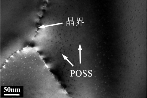
Nano-sized POSS-TriSilanolCyclohexyl particles near the grain boundary of Sn-3.5Ag.
Nano-sized POSS-TriSilanolCyclohexyl particles near the grain boundary of Sn-3.5Ag.
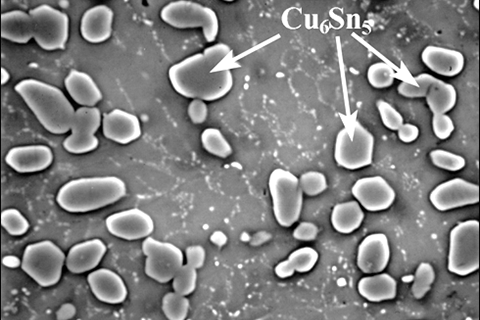
Cu6Sn5 IMC particle reinforced Sn-3.5Ag composite solder, fabricated by in-situ method.
(2) High temperature interconnect materials
Traditional interconnect materials are difficult to meet the demands of high temperature and multistage packaging with the development of modern information industries. Due to the low-temperature sintering and high-temperature service characteristics, nanoparticle pastes are most likely to be the potential interconnect materials for high temperature and multistage packaging. For the research and development of nanoparticle pastes, the research areas include: (1) the preparation and sintering behavior of Cu NPs pastes, Ag NPs pastes and Cu@Ag micro/nano particle pastes; (2) the surface nanocrystallization of substrate and the analysis of its sintering interface with nanoparticle pastes.
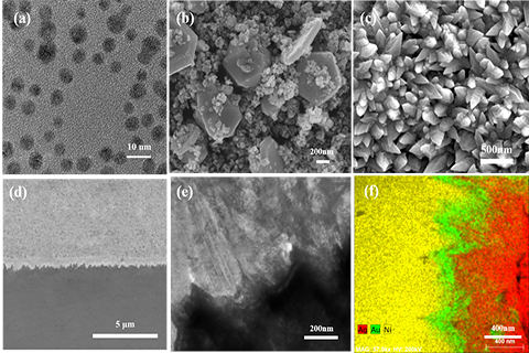
(a) TEM images of Ag NPs; (b) SEM images of Cu@Ag micro/nano particles; (c) SEM images of Ni nanoarray film; (d) SEM images of sintered interface between Ag NPs and Ni/Au nanoarray film; (e,f) TEM images of sintered interface between Ag NPs and Ni/Au nanoarray film and corresponding element mapping
Service reliability of interconnect materials and structures
Solders are important interconnect and structural materials in microelectronic packages, where signal transmission and structural support are their basic roles. Once a new type of solder material is prepared, the reliability of solder joint is essential to ensure its service capability. The service conditions for solder joints are getting increasingly severe with the miniaturization of the packages. These conditions are often induced by cyclic loading through environmental temperature excursions, applied external high current density, impact loading from hitting obstacles, low temperature storage, high temperature aging, etc. The single parameter of various reliability concerns, such as aging, creep, themomechanical fatigue, electromigration, thermo-migration, Sn-whisker growth, Sn-pest, etc., was investigated and characterized separately. Recent complex service scenarios have also enabled a series of study of the coupled effects from various reliability parameters, such as creep and current stressing, mechanical, electric and thermal stressing, etc. A complete set of testing and analytical design methodology, experimental setup, characterization, and modeling techniques was built in the lab, for either real-time or in-situ observation and analysis.
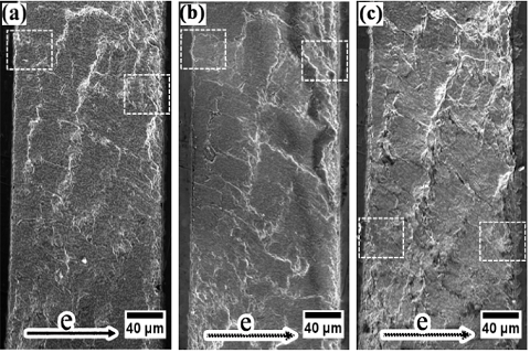
Microstructure evolution of simple shear Sn58Bi solder joint under 5×10²A/cm2 current density and thermal cycling. (a) TC20 (b) TC40 (c) TC80
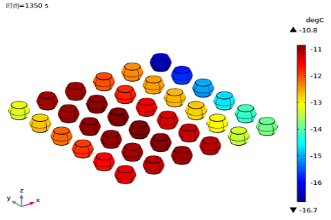
Physical Parameters Distribution of Sn3.0Ag0.5Cu solder joints under the applied current stressing for 1350s and 0.05V Voltage
Fundamentals studies on mechanisms of material behavior in electronic packaging interconnects
As representative interconnect materials, solders have exhibited classic metallic materials behavior showing the entangled relationship among structure, property, processing and performance. Being the core member of the interconnect structure, solder joint is also constrained by the way how interconnect interfaces are established, what other component materials are involved, etc. Therefore, fundamental material properties and behavior need to be revisited to reveal their true nature. We have been focused on the fundamental studies of solders and their joints, as constrained by their processing and applications. Issues we have paid special attentions include melting and wetting, non-equilibrium solidification, kinetics of IMC growth, bulk and interfacial diffusion, creep mechanisms, grain boundary behavior, strengthening mechanisms, phase stability, and so on. In the microscopic failure of solder joints under thermal fatigue, electromigration, we have discussed the microscopic processes of subcrystalline rotation, dislocation multiplication, and grain refinement during thermal fatigue, and explored the effects of intermetallic compound growth and the number of Sn grains on electromigration behavior, which lays a theoretical foundation for mitigation of the disastrous effects from thermal and electromigration induced failure.
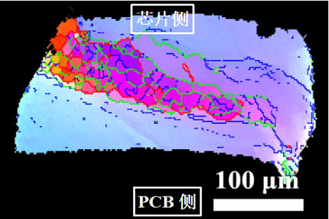
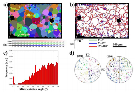
EBSD map of the solder joint after 900 thermal shock cycles showing different Sn grain orientation.
Growth model of intermetallic compound particles in Sn-based solder joint under electromigration.
New Interfacial Layer Materials
The reliability of micro solder joints in electronic packaging does not only depend on the performance and service performance of the solder, but the effective combination of the solder and the pad at the interface is the key to reliable connection. The inter-diffusion of elements on the pad side and the solder side will generate intermetallic compound layers (IMCs) that are unfavorable for bonding, which will greatly affect the thermal, mechanical, and electrical properties at the interface. The industry will introduce an interface layer between the pad and the solder to play three roles: diffusion barrier, wetting, and bonding. The common interface layer uses Ni-based, silver-based, organic solderability preservative (OSP), etc., but there will always be some weaknesses under long-term service. For example, Ni-based materials have a fast reaction rate, silver-based materials are easy to oxidize, and organic protective film materials need to be stored in a vacuum and have a short shelf life. The Co-P-based interface layer, as a high-quality metal film material that has gradually attracted the attention of the academic community, can overcome the above three shortcomings, and the Co-Sn compound formed with the solder shows better mechanical properties. Our research group has carried out in-depth research on the preparation process, interface diffusion, service reliability and other issues of Co-P interface layer materials.
(1) The effect of P content on the structure and properties of Co-P interface layer materials.
A series of 0-21at.%P Co-P films were prepared, and the phase composition was determined by XRD. Provide support for the study of P element on the deposition mechanism of Co.
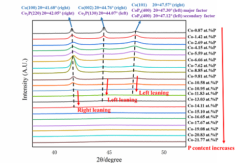
XRD spectra of the Co–P films with different P contents
(2) Co-P composition point and mechanism of the best performance in barrier diffusion.
Through the aging experiment of Cu/Co-P/SnAg diffusion couple with 0-21at.%P, systematically explore the IMC difference at the interface and IMC crystal structure under different P content, It provides a theoretical basis for the study of the optimal interface layer composition under constant temperature aging conditions.
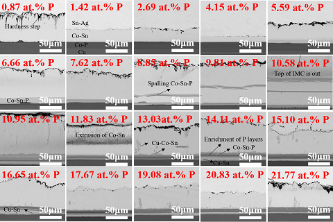
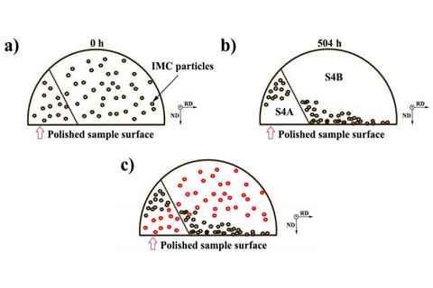
Interfacial reaction and diffusion in the Sn–Ag /Co–x at.% P (x=0.87~21.77)/Cu joints.at 453K remaining for 120 hours.
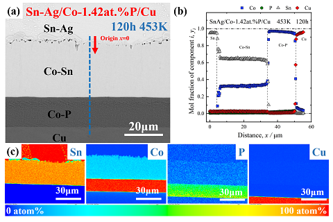
Interfacial reaction and diffusion in the Sn–Ag /Co–1.42 at.% P /Cu joints.at 453K remaining for 120 hours. (a) Image of backscattered electrons of IMCs structure, (b) Line-scanning EPMA results of atomic percentage of Co, P, Sn, Cu.in the blue-line region (c) Area-scanning EPMA results of Co, P, Sn, Cu in area of (a).
(3) Service behavior and failure mechanism of solder joints containing Co-P interface layer under severe loads
Our research group plans to start the reliability study of the interface layer after completing the study of the best diffusion barrier composition point, including but not limited to severe loads such as electro-migration, thermal fatigue, and shear creep of the solder joints containing the interface layer.
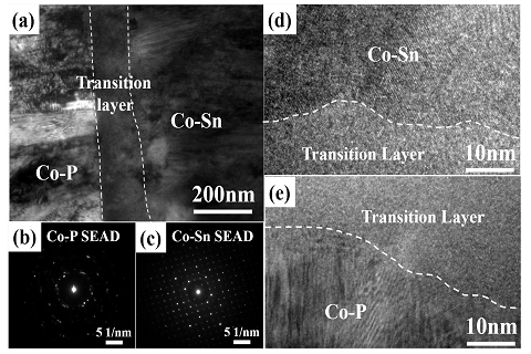
TEM analysis at the interface of Co-Sn/Co-P in the Sn–Ag/Co–1.42 at.% P joint at 453K remaining for 120 hours. (a) TEM image at the interface, (b) Selected Area Electron Diffraction of Co-P, (c) Selected Area Electron Diffraction of Co-Sn, (d) HRTEM image at interface of the Co-Sn and the transition layer, (e) HRTEM image at the interface of the Co-P and the transition layer.
We are currently still working hard on several projects in this area called upon various scenarios and stakeholders. We have a lot of classic publications and monographs from our significant research findings in the past two decades, which we believe has cumulated significant amount of knowledge and expertise. Welcome to join us for this fantastic area in the age of 5G.
Representative Publications:
- F. Guo, “Composite lead-free electronic solders”, J Mater Sci: Mater Electron, volume 18, Numbers 1-3, ISSN 0957-4522 March 2007, pp.129
- B. Li, Y. Shi, Y. Lei, F. Guo, Z. Xia, and B. Zong, “Effect of rare earth element addition on the microstructure of Sn-Ag-Cu solder joint”, Journal of Electronic Materials, 34(3), 217(2005)
- F. Guo, M. Zhao, Z. Xia, Y. Lei, X. Li, and Y. Shi, “Lead-free solders with rare earth additions”, JOM, 61(6), 39(2009).
- G. Xu, H. He, and F. Guo, “Temperature-Dependent Phase Segregation in Cu/42Sn-58Bi/Cu Reaction Couples under High Current Density”, Journal of Electronic Materials, 38(2), 273(2009).
- F. Guo, G. Xu, H. He, M.Zhao, J. Sun, and C. H. Wang, “Effect of Electromigration and Isothermal Aging on the Formation of Metal Whiskers and Hillocks in Eutectic SnBi Solder Joints and Reaction Films”, Journal of Electronic Materials, 38(12), 2647(2009).
- R. Zhang, G. Xu, X. Wang, F. Guo, A. Lee, and K.N. Subramanian, “Electromigration in Sn-Bi modified with polyhedral oligomericsilsesquioxane”, Journal of Electronic Materials, 39(12), 2513(2010).
- F. Tai, F. Guo, J.P. Liu, Z.D. Xia, Y.W. Shi, Y.P. Lei, and X. Li, “Creep properties of Sn-0.7Cu composite solder joints reinforced with nano-sized Ag particles”, Soldering and Surface Mount Technology, 22(4), 50(2010).
- L. Ma, F. Guo, G. Xu, X. Wang, H. He, and H. Zhao, “Investigation of Stress Evolution Induced by Electromigration in Sn-Ag-Cu Solder Joints Based on an X-Ray Diffraction Technique”, Journal of Electronic Materials, 2012, 41(2): 425-430
- S. Liu, L. Ma, Y. Shu, K. Subramanian, A. Lee, F. Guo, “Effects of POSS-Silanol Addition on Whisker Formation in Sn-Based Pb-Free Electronic Solders”, Journal of Electronic Materials, 2014, 43(1): 26-32
- J. Han, S. Tan, F. Guo, “Study on Subgrain Rotation Behavior at Different Interfaces of a Solder Joint During Thermal Shock”, Journal of Electronic Materials, 2016, 45(12): 1-9
- J. Han, F. Guo, J. Liu, “Early stages of localized recrystallization in Pb-free BGA solder joints subjected to thermomechanical stress”, Journal of Alloys and Compounds, 2017, 704(15): 574-584
- Y. Wang, J. Han, Y. Wang, L. Ma, F. Guo, “Effect of the Angle Between Sn Grain c -Axis and Electron Flow Direction on Cu-Reinforced Composite Solder Joints Under Current Stressing”, Journal of Electronic Materials, 2018, 47(1): 96-102
- Y. Zuo, T. R. Bieler, Q. Zhou, L. M. Ma, F. Guo, “Electromigration and Thermomechanical Fatigue Behavior of Sn0.3Ag0.7Cu Solder Joints”, Journal of Electronic Materials, 2018, 47(3): 1881-1895
- Y. Tian, L. Ma, Y. Wang, et al., ” The Growth of Interfacial IMC Layer in SAC0307 Solder Joints with Specific Grain Orientation Under Electrical and Thermal Coupling Fields”, Journal of Electronic Materials, 2020, 49(1):202-211.
- Zhou W , Zheng Z , Wang CQ , et al. One-Step Fabrication of 3D Nanohierarchical Nickel Nanomace Array To Sinter with Silver NPs and the Interfacial Analysis. ACS Applied Materials & Interfaces, 2017, 9(5):4798–4807.